A B B C Circuit Diagram
6 bc547 simple circuits Draw logic circuit diagram for the following expression: y=ab + b`c+c`a Equivalent simulated
Solved Derive the SOP expression for the logic circuit given | Chegg.com
Notes for/from class Ab nand only circuit logic diagram draw using gates input Circuit notes diagram class anh luc cs edu
Ab breadboard circuit logic inputs placed creating basic ac digital electronics imply trying should don know re look stack
Solved derive the sop expression for the logic circuit givenAbc bc mn Circuits diagrams circuit1 peoiLogic sop circuit expression bc given derive ab ac abc solved below chegg problem part.
Draw the circuit diagram for f = ab’c + c’b using nand – to – nandChapter 7 section c re-drawing complex schematics Boolean expression following circuit diagram given ab truth draw table logic bc construct solved derive chegg useLogic questions.

Electronics circuit diagram
(a) layout, (b) equivalent circuit, and (c) simulated results of theDigital logic Section 2 homework[diagram] circuit diagram boolean expression ab c d.
Draw logic circuit diagram for the following expression: y=ab + b`c+c`a .

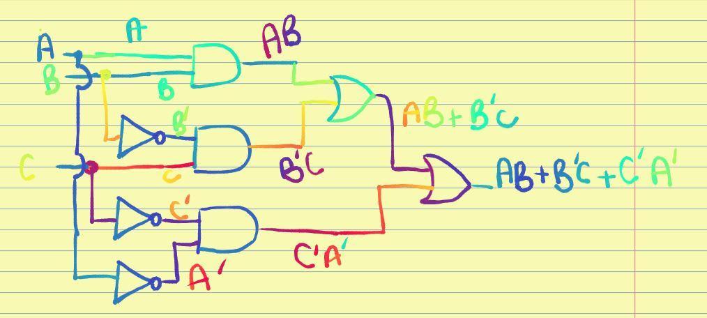
DRAW LOGIC CIRCUIT DIAGRAM FOR THE FOLLOWING EXPRESSION: Y=AB + B`C+C`A

DRAW LOGIC CIRCUIT DIAGRAM FOR THE FOLLOWING EXPRESSION: Y=AB + B`C+C`A
![[DIAGRAM] Circuit Diagram Boolean Expression Ab C D](https://i2.wp.com/d2vlcm61l7u1fs.cloudfront.net/media/d62/d624186d-8915-4675-bbd6-6b0f80ba6bcd/phpYTHfqV.png)
[DIAGRAM] Circuit Diagram Boolean Expression Ab C D

Draw the circuit diagram for F = AB’C + C’B using NAND – to – NAND

(a) Layout, (b) equivalent circuit, and (c) simulated results of the

digital logic - Creating a basic ab + a'c circuit on a breadboard, how

Section 2 Homework

Solved Derive the SOP expression for the logic circuit given | Chegg.com

Chapter 7 Section C Re-drawing complex schematics

Electronics